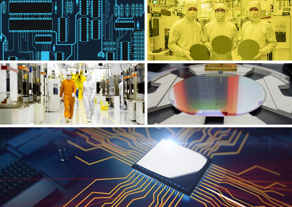
In the intricate world of semiconductor manufacturing, precision and reliability are paramount. One crucial but often overlooked component in this process is the humble test wafer. Test wafers play a pivotal role in ensuring the quality and functionality of semiconductor devices, serving as miniature laboratories for the semiconductor industry.
In this blog post, we will delve deep into the science behind test wafers, shedding light on their composition, fabrication, evaluation parameters, and the impact of defects. We will also explore techniques for characterizing performance, offer optimization tips, present real-world case studies, and discuss the challenges and advancements in test wafer technology. Join us on this enlightening journey into the heart of semiconductor manufacturing.
Materials and Layers
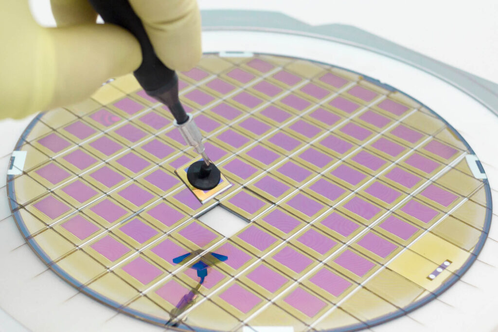
Test wafers, often made of silicon, are thin, circular substrates that mimic the wafer used in semiconductor production. These patterned silicon wafers undergo a series of intricate processes to replicate the essential layers found in the final semiconductor product. Silicon is chosen due to its semiconductor properties and compatibility with the manufacturing process.
To mimic the device’s layers, insulating materials like silicon dioxide and conducting materials like polysilicon are deposited onto them. These layers are then patterned using techniques like photolithography to resemble the circuits found in real devices. They can also feature specialized layers for testing specific attributes, such as stress sensors or probe pads for electrical testing.
Semiconductor Manufacturing
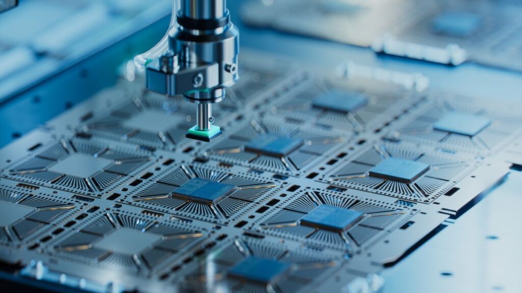
The significance of test wafers lies in their ability to act as proxies for the final semiconductor devices. They are utilized at various stages of manufacturing, from research and development to process optimization and quality control. They help semiconductor manufacturers validate their processes, assess equipment performance, and ensure the integrity of their designs.
They also serve as valuable tools for characterizing the effects of different process variations and deviations. Essentially, they are the litmus test for the entire = manufacturing ecosystem, allowing engineers to fine-tune their processes and deliver high-quality, reliable chips to the market.
Understanding the Fabrication Process
Creating them is a meticulous process that mirrors many steps of actual semiconductor fabrication. It begins with the selection of a high-purity silicon wafer as the substrate. This wafer undergoes cleaning, polishing, and doping processes to ensure it meets the desired specifications. Next, multiple layers of materials are deposited onto the wafer using techniques like chemical vapor deposition (CVD) and physical vapor deposition (PVD).
Photolithography and etching steps follow, allowing for the precise patterning of circuits and structures. Finally, they may undergo various thermal treatments to achieve the desired electrical properties. This intricate process ensures that they faithfully mimic the conditions of actual devices.
Key Parameters for Evaluating Quality
To assess the reliability and accuracy, several key parameters come into play. These parameters include thickness uniformity, surface roughness, defect density, electrical characteristics, and material composition. Thickness uniformity ensures that the layers on them are consistent, preventing variations in testing results. Surface roughness affects the quality of photolithography, which is critical for patterning.
Defect density is a crucial metric, as high defect levels can skew testing results. Electrical characteristics are assessed to ensure they behave similarly to the final product. Material composition verification confirms that the layers accurately mimic those in devices. Maintaining stringent control over these parameters is essential for reliable testing.
Analyzing the Impact of Defects
Defects are the nemesis of semiconductor manufacturing, and they are no exception. Even minor defects can lead to inaccurate testing results and unreliable data. Defects can take various forms, including particles, scratches, and irregularities in material deposition. These imperfections can interfere with electrical measurements, introduce noise into testing data, and even lead to false positives or negatives.
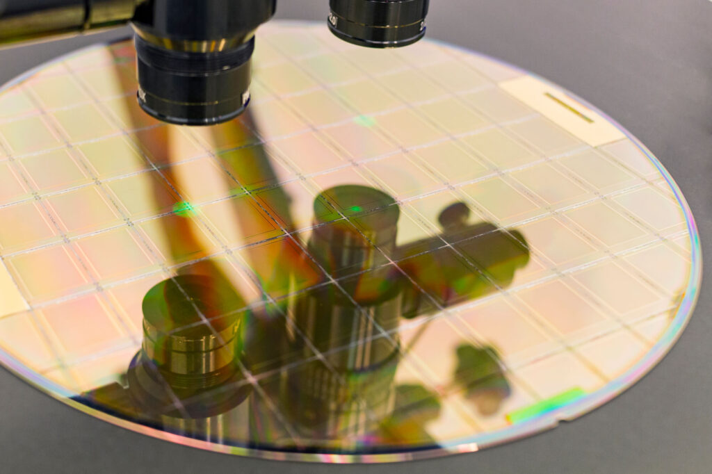
Detecting and mitigating defects on them is an ongoing challenge in semiconductor manufacturing. Advanced inspection techniques, such as scanning electron microscopy (SEM) and atomic force microscopy (AFM), are employed to identify and analyze defects, allowing manufacturers to improve the quality.
Techniques for Characterizing Performance
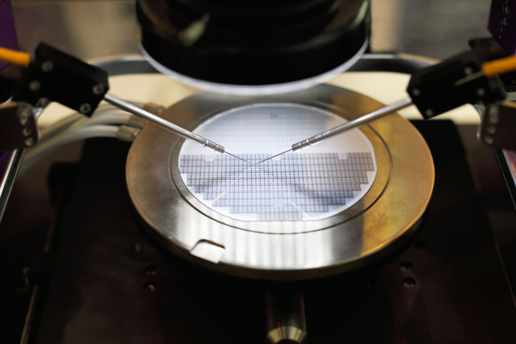
Characterizing their performance involves a suite of sophisticated techniques that provide insights into their behavior under different conditions. Electrical testing, including measuring resistance, capacitance, and impedance, is a fundamental approach. This helps verify that the electrical properties align with the final semiconductor device. Additionally, stress tests are conducted to assess how they behave under extreme conditions, such as high temperatures or mechanical stress. Optical techniques, such as spectroscopy and ellipsometry, are used to analyze the test wafer’s optical properties.
Tips for Optimizing Testing Procedures
Optimizing test wafer testing procedures is critical for efficiency and accuracy in semiconductor manufacturing. To achieve this, it’s essential to establish clear testing protocols, ensuring consistency and repeatability across different batches of test wafers. Regular calibration of testing equipment is paramount to maintain accuracy. Moreover, real-time monitoring and data analysis during testing can identify anomalies and trends, allowing for timely adjustments.
Collaborative efforts between engineers and equipment suppliers can lead to innovative testing solutions. Additionally, incorporating machine learning and artificial intelligence algorithms into data analysis can enhance predictive maintenance and optimize testing processes.
Case Studies Showcasing Successful Applications
To illustrate the real-world impact of test wafers, let’s explore a few case studies where their use has been instrumental. In one instance, a semiconductor manufacturer used test wafers to validate a new lithography process, ensuring that it met stringent resolution requirements. Another case study involved using them to optimize chemical mechanical polishing (CMP) processes, resulting in a significant reduction in defect density in the final product.
They have also been invaluable in characterizing the performance of emerging materials, such as gallium nitride (GaN) for high-power devices, enabling their successful integration into semiconductor manufacturing.
Challenges and Advancements in Technology
Despite their critical role, they face several challenges in the ever-evolving semiconductor industry. As semiconductor devices become smaller and more complex, they must keep pace with the shrinking feature sizes and increasing demands for accuracy.
Ensuring that they accurately mimic the behavior of advanced semiconductor materials and structures is an ongoing challenge. Advancements in materials science, nanotechnology, and process technology continue to influence development, with innovations such as 3D test structures and advanced materials becoming increasingly relevant.
Conclusion: The Future in the Semiconductor Industry
In conclusion, they are unsung heroes in the semiconductor manufacturing process, enabling the industry to achieve precision, reliability, and innovation. Their composition, fabrication, and characterization are crucial for quality control and process optimization. They play a pivotal role in detecting defects, ensuring the accuracy of electrical measurements, and validating new processes and materials.
As the semiconductor industry continues to advance, so too will the role and technology. With ongoing research and development, they will remain a linchpin in semiconductor manufacturing, contributing to the production of cutting-edge devices that power our modern world.